
Compared to many years ago, mobile consumer electronic devices are complex and feature-rich, capable of storing large amounts of music, photos, and video content. The good news is that the storage system architecture can accommodate these new data-intensive applications. For example, cost-effective compact NAND flash for mass storage replaces NOR flash and other non-volatile storage used in cell phones, MP3 players and digital cameras.
As process technology advances, the memory density doubles approximately every 12 to 18 months. For NAND flash, this means an increasing emphasis on multi-level cell (MLC) technology. Traditional single-level cell (SLC) NAND flash memory can store one bit of data per storage unit. MLC technology enables multiple data bits to be stored in a single memory cell, with data storage capacity up to twice that of the same size NAND flash device. MLC NAND further accelerates the cost per byte of NAND flash and provides room for new applications. Market trends indicate that shipments of MLC flash memory surpassed SLC flash memory in early 2007.
With the adoption of MLC NAND, the shortening of the NAND product cycle has made the work of system designers more and more complicated. Traditional SLC NAND flash requires only one bit of error check code per 512 bytes, and most new embedded processors can support it directly. Today's MLC flash devices are different, requiring a 4-bit check code per 512-byte sector. Future MLC NAND requirements for ECC will exceed 8-bit parity for every 512-byte sector. The implementation of advanced ECC algorithms and hardware acceleration circuits pose significant challenges to the design of embedded processors and host systems.
System designers must also be able to cope with the rapid update of NAND flash and the challenges of product functionality differences between different vendors. System designers and processor manufacturers must invest more in hardware and software development to keep pace with NAND flash manufacturers. More importantly, additional development work can have a significant impact on time to market.
The right solution is to use Micron's innovative managed NAND products. Managed NAND flash combines Micron's high-quality, low-cost NAND flash memory with a half-height, high-speed MulTIMediaCard. (MMC) controller with a JEDEC-compliant BGA package and an advanced 10-signal interface.
MMC is a high-performance interface with outstanding features that is supported by almost all embedded processors in wireless consumer electronics applications. If an 8-bit data bus and standard BGA are used, the managed NAND supports an interface rate of 52 MB/sec (peak). Because the processor's interface does not change, the underlying NAND technology in the BGA can be changed without affecting the application. This approach extends the life of higher density solutions to support multiple component densities through a system board design.
Another major advantage of manageable NAND is the elimination of reliance on specific vendor flash firmware and drivers on the host processor (this dependency makes the host processor need to coordinate program/erase/read functions and manage bad blocks and Bad bits) thus making standard NAND a simple read and write device. The host processor does not have to consider unnecessary NAND function details such as NAND block size, page size, new features, process generation, MLC and SLC, average read and write algorithms, and ECC requirements. The industry-standard universal MMC device driver allows the processor to work seamlessly with Micron Managed NAND and other vendors' products that meet the same standards.
The concept of manageable NAND devices has been proposed as an industry standard to be accepted. The
MulTIMediaCard AssociaTIon and JEDEC jointly announced the use of eMMC. as the name and trademark of this category of flash memory devices in December 2006.
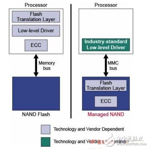
Figure 1: NAND flash configuration manages NAND functions
Manageable NAND is an all-in-one memory and controller device with an MMC interface. It complies with the MMC system specification version 4.2 and is fully compatible with MMCplus., MMCmobile., MMCmicro. and past MMC.
The main function:
. Can support both MMC and SPI mode operation
. Hosts can choose x1, x4 and x8 I/O
. . 52 MHz clock speed (highest)
. . 416 Mb/s (52 MB/s) data rate (highest)
. 3.3V and 1.8V working voltage
. .password protection
. .Permanent and temporary write protection
. Internal ECC, average read and write algorithms, and block management.
The JEDEC standard BGA package with manageable NAND has the potential to integrate other memory components such as DRAM to help system designers implement highly integrated system memory solutions.
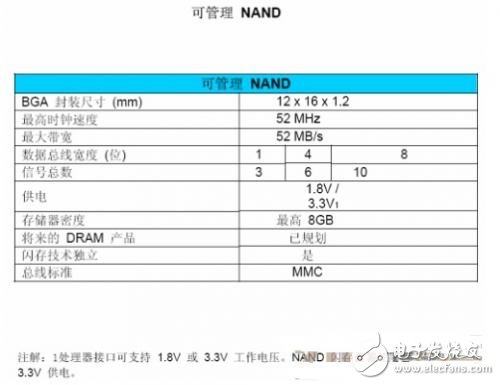
Table 1: Manageable NAND Attributes
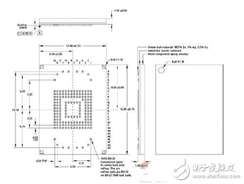
Figure 2: Manageable NAND package details
Note: Dimensions are in millimeters.
The lowest bill of materials (BOM) cost can be achieved if the host processor can interface directly with standard NAND flash. Unless the processor has built-in support for NAND, the operational complexity of NAND flash can be a headache for system designers.
A relatively simple SLC NAND flash ECC algorithm can be implemented in software, but higher performance applications require hardware support. Future MLC devices will require more sophisticated ECC and block management capabilities, and will continually attach requirements to the processor support hardware.
When choosing a NAND solution, system designers should consider development resources and whether there is a match between system performance and application requirements. Does the development team have software development resources and have NAND memory block management software code? Does the embedded processor selected for the project have ECC functionality for NAND devices? If so, does ECC support the larger bit verification requirements required for MLC NAND flash and whether it has sufficient performance for the application.
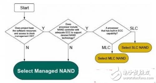
Figure 3: NAND memory selection tree
Industrial Switches,Gigabit Ethernet Switch,12 Port Industrial Switch,Managed Switches 8 Port
Shenzhen Scodeno Technology Co.,Ltd , https://www.scodenonet.com