In some places where high voltage and low current are required, a voltage doubler rectifier circuit is often used. Double voltage rectification can lower the AC voltage and use a high-voltage rectifier diode and capacitor to “finish†a higher DC voltage. The voltage doubler rectifier circuit is generally divided into two voltage, three voltage and multiple voltage rectifier circuits according to how many times the output voltage is the input voltage.
The working principle of voltage doubler rectifier circuit: 1. Principle of voltage doubler rectifier circuit1) In the negative half cycle, when A is negative and B is positive, D1 is turned on and D2 is turned off. The power supply is charged to capacitor C1 via D1. In an ideal case, D1 can be regarded as a short circuit and capacitor C1 is charged during this half cycle. To Vm, its current path and the polarity of capacitor C1 are as shown in Figure (a). RJy838 Electronic-Technical Data-Electronic Components-Circuit Diagram-Technology Application Website-Basic Knowledge-Principle-Maintenance-Action-Parameter-Electronic Component Symbol
(2) When the positive half cycle, that is, A is positive and B is negative, D1 is cut off and D2 is turned on. The power supply is charged to C2 via C1 and D1. Since Vm of C1 is added to Vm of the secondary side of the double press, c2 is made. Charging to the highest value of 2Vm, the current path and the polarity of capacitor C2 are as shown in Figure (b). In fact, the voltage of C2 can't be charged to 2Vm in one and a half weeks. It must gradually approach 2Vm after a few weeks. For the convenience of explanation, the following circuit description also makes this assumption. If a half-wave voltage multiplier is used in a power supply without a transformer, we must connect C1 in series with a current limiting resistor to protect the diode from damage from the beginning of the charging current. If there is a load connected in parallel to the output of the voltage doubler, as expected, the voltage on capacitor C2 will decrease in the negative half cycle (in the input), and then be charged to 2Vm in the positive half cycle as shown below. Shown.
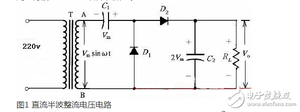
Figure 1 DC half-wave rectification voltage circuit
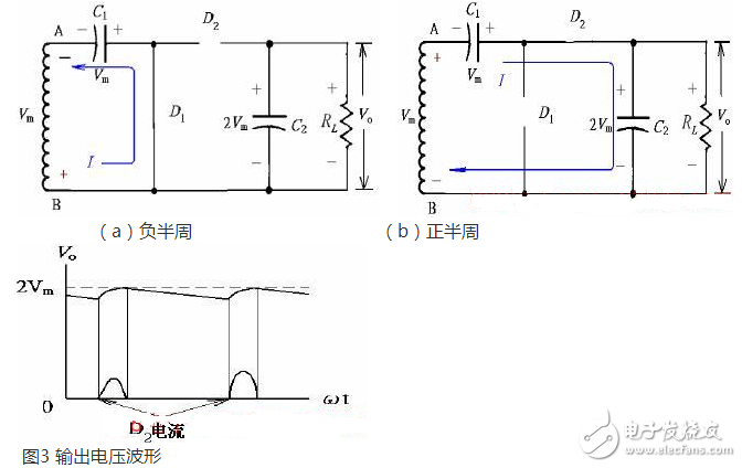
Therefore, the voltage waveform on the capacitor c2 is a half-wave signal filtered by the capacitance filter, so the voltage multiplying circuit is called a half-wave voltage circuit.
In the positive half cycle, the maximum reverse voltage of diode D1 is 2Vm. When the negative half wave is used, the maximum reverse voltage value of diode D2 is also 2Vm. Therefore, the diode of PIV 》2Vm should be selected in the circuit.
2, full wave voltage doubler circuit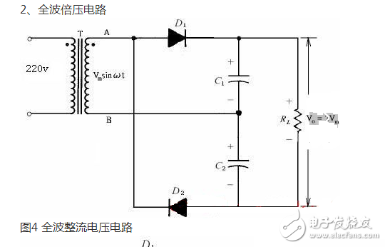
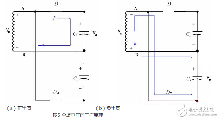
In the positive half cycle, D1 is turned on, D2 is turned off, and capacitor C1 is charged to Vm, and the current path and the polarity of the capacitor C1 are as shown in the above (a).
In the negative half cycle, D1 is turned off, D2 is turned on, capacitor C2 is charged to Vm, and the current path and the polarity of the capacitor C2 are as shown in the above (b).
Since C1 and C2 are connected in series, the DC voltage is output, and V0=Vm. If no load current is drawn from the circuit, the voltage across capacitors C1 and C2 is 2Vm. If the load current is drawn from the circuit, the voltage across capacitors C1 and C2 is the same as the voltage across a capacitor fed by the full-wave rectification circuit. The difference is that the effective capacitor is the series capacitor of C1 and C2, which is smaller than C1 and C2 alone. This lower capacitance value will make its filtering less effective than a single capacitor filter circuit.
In the positive half cycle, the maximum reverse voltage of diode D2 is 2Vm. When the negative half cycle, the maximum reverse voltage of diode D1 is 2Vm, so the diode of PVI 》2Vm should be selected in the circuit.
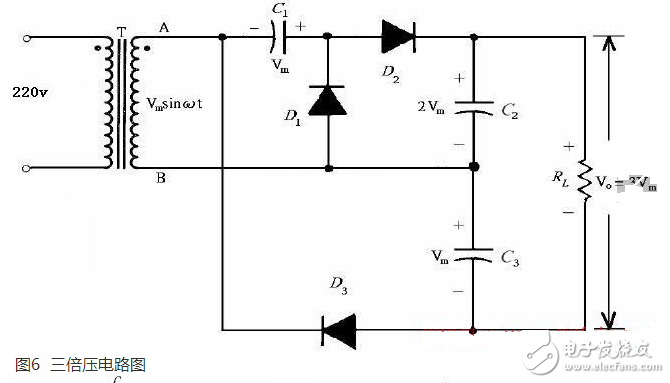
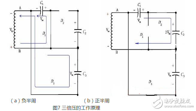
During the negative half cycle, D1 and D3 are turned on, D2 is turned off, and capacitors C1 and C3 are all charged to Vm. The current path and the polarity of the capacitor are as shown in (a) above.
In the positive half cycle, D1 and D3 are turned off, D2 is turned on, and capacitor C2 is charged to 2Vm, and the current path and the polarity of the capacitor are as shown in the above (b).
Since C2 is connected in series with C3. Therefore, the output DC voltage V0=3m.
In the positive half cycle, the maximum reverse voltage of D1 and D3 is 2Vm. When the negative half cycle, the maximum reverse voltage of diode D2 is 2Vm, so the diode of PIV 》2Vm should be selected in the circuit.
4, N times voltage roadThe generalized form of the half-wave voltage doubling circuit in the figure below, which produces three or four times the input peak value. According to the hairline of the line connection, if the additional diodes and capacitors are connected, the output voltage will become five, six, seven, or even more times the basic peak (Vm). (ie N times)

During the negative half cycle, D1 is turned on, the other diodes are turned off, and the capacitor C1 is charged to Vm, and the current path and the polarity of the capacitor are as shown in (a).
In the positive half cycle, D2 is turned on, the other diodes are turned off, and the capacitor C2 is charged to 2Vm, and the current path and the polarity of the capacitor are as shown in the above (b).
During the negative half cycle, D3 is turned on, the other diodes are turned off, and the capacitor C3 is charged to 2Vm, and the current path and the polarity of the capacitor are as shown in the above (c).
In the positive half cycle, D4 ​​is turned on, the other diodes are turned off, the capacitor C4 is charged to 2Vm, and the current path and the polarity of the capacitor are as shown in the above (d).
Therefore, from the top of the transformer winding, an odd multiple of Vm can be obtained at the output. If the voltage is measured from the bottom of the winding of the transformer, the output voltage will be an even multiple of Vm of the peak voltage.
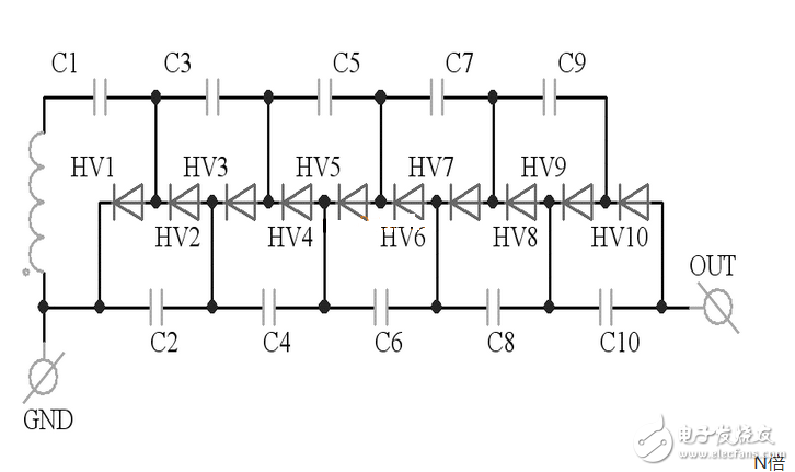
N voltage rectification circuit diagram
Double voltage rectification, this circuit is charged in parallel, series discharge to obtain N times higher than the input voltage. Suitable for applications requiring high voltage and low current.
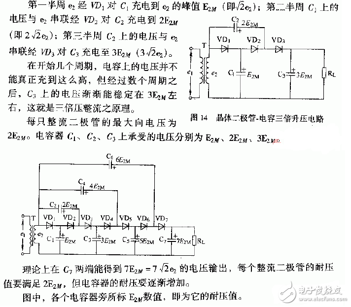
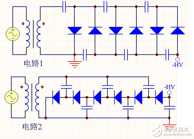

These three circuits are all 6 times voltage rectifier circuits, each with its own characteristics. We usually say that every 2 times is the first order, denoted by N, the above circuits are all 3 orders, that is, N=3. If you want the output voltage to be different in polarity, just reverse all the diodes.
The advantage of circuit 1 is that the voltage on each capacitor does not exceed twice the secondary peak voltage U of the transformer, ie 2U, so a capacitor with a lower withstand voltage can be selected. The disadvantage is that the capacitor is in series discharge and the ripple is large.
The advantage of the circuit 2 is that the ripple is small, and the disadvantage is that the voltage withstand voltage of the capacitor is high, and as the N increases, the voltage stress of the capacitor increases. The voltage of the last capacitor in the figure reaches 6U.
Circuit 3 is an improvement of circuit 1. The advantage is that the ripple is much smaller than circuit 1, and the voltage stress of the capacitor does not exceed 2U. The disadvantage is that the circuit is complicated.
The circuit 1 is taken as an example to briefly explain the working principle: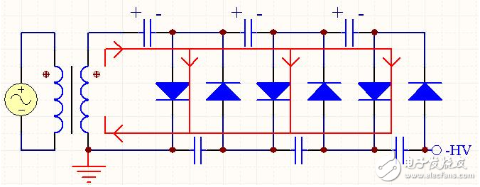
When the secondary output of the transformer is up and down, the current flows as shown. The transformer charges energy to the three capacitors of the upper arm.
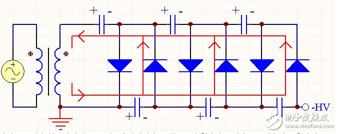
When the secondary output of the transformer is up-down, the current flows as shown. The upper arm capacitor is charged through the secondary arm of the transformer.
If there is no load, in steady state, except for the leftmost capacitor, the voltage on each of the other capacitors is 2U, so the total output voltage is 6U. In fact, due to the poor carrying capacity of the high-order voltage doubler rectifier circuit, the output of a small power will cause a large drop in the output voltage. Assuming that the output current is I, the capacity of each capacitor is the same, C, and the AC power frequency is f, then the voltage drops to:

The output voltage ripple is:

The high-voltage power supply of the general-purpose oscilloscope includes one positive high-voltage two-way negative high voltage, and the circuit adopts “high-frequency high-voltage†mode. The basic circuit is shown in Figure 3. BG1, L1, L2 and C1 form a high-frequency oscillator. The oscillating signal rises at L3 and L4, and is rectified by C3~C7 and BG7~BG11. After R1 and C10 are filtered, the positive high voltage supply is accelerated to form an anode. BG6 half-wave rectification, C8, C9 and R2π type filtering, to obtain a negative high voltage supply cathode.
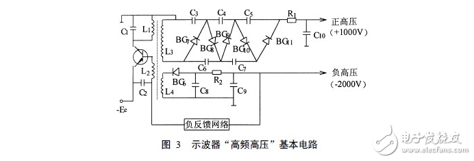
The oscilloscope's high frequency, high voltage and display circuits are a key part of the instrument. Only the working voltage of each electrode in the oscilloscope meets the rated condition to form a signal waveform to be observed by the ideal electron beam scanning. The accuracy and stability of the high voltage value directly affects the sensitivity of the X and Y amplifiers. The common faults of high-voltage circuits are: no light point, no high-voltage oscillation, poor focus, no brightness, darkness, pattern distortion, and the screen display waveform amplitude changes with brightness when the brightness potentiometer is adjusted. There are many reasons for these failures. Only high-voltage circuit faults are analyzed and eliminated.
(1) Detection method. There are two kinds of detection methods for oscilloscope display circuit high voltage (above 1kV): use a multimeter with a high voltage bar with a DC voltage range greater than 10,000 to directly measure; by empirical observation and estimation, the method is: first disconnect the power supply, from the oscilloscope Remove the high pressure cap from the high pressure nozzle, hold the high voltage wire (as far as possible from the high pressure cap), then turn on the power supply, and slowly move the high voltage wire so that the high pressure cap approaches the high pressure nozzle, about one centimeter away from the high pressure nozzle, start pulling Arc discharge, if the sound of "啪, 啪, 啪" is issued, it indicates that the high pressure is basically normal.
(2) Fault phenomenon and repair. (Phenomenon: the spot flashes). This fault is usually caused by high-pressure sparking. First, check the high-pressure nozzle from the appearance, and find that the high-pressure cap is aging and partially broken. After the replacement, the fault still exists. Listening carefully to the body, you can hear the sound of high-voltage discharge, according to the severity of the sound of the fire, it is preliminarily determined that the sound of the fire is transmitted from the high-pressure sleeve. Fold down the high-voltage sleeve to take out the voltage doubler rectifier board. In the case of power failure, use the multimeter R&TImes; 10kΩ file to measure the six silicon stacks (2DL5/0.2) on the circuit board are normal. Then turn on the power and measure six high-voltage capacitors (6 800P/3kV) with a multimeter with a multimeter voltage of 2 500V. It is found that the measured voltage value across the capacitor C3-16 swings with the occurrence of the ignition sound. From the outside, it was found that the insulating case of this capacitor fell off a small piece due to high-voltage ignition. After changing this capacitor, the high voltage does not ignite, and the phosphor screen spot is stable.
Only a low-voltage AC power supply and a low-voltage rectifying component, and a DC voltage higher than the rectified input voltage several times, a double-voltage rectification circuit can be used, but its load capacity is poor, and it is only suitable for DC high-voltage and small current. Medium power rectification. When the rectifier circuit is selected, it is necessary to pay attention to the relationship between the average current ID flowing through the diode and the load current, the relationship between the reverse peak voltage of the diode and the secondary voltage of the transformer, and the withstand voltage of the capacitor.
Double voltage rectification electronic ballast circuit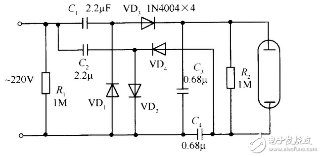
Twinkle System Technology Co Ltd , https://www.pickingbylight.com
