
Introduction
The classic four-resistance differential amplifier (Different Timal Amplifier) ​​seems simple, but its performance in the circuit is not good. Starting from the actual production design, this paper discusses the shortcomings of discrete resistance, filtering, AC common mode rejection and high noise gain.
The electronics course at the university illustrates the application of an ideal op amp, including inverting and non-inverting amplifiers, which are then combined to build a differential amplifier. The classic four-resistor differential amplifier shown in Figure 1 is very useful, and has been introduced in textbooks and lectures for more than 40 years.
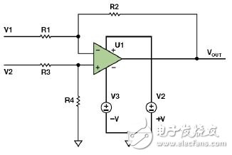
Figure 1. Classical Difference Amplifier
The transfer function of this amplifier is:
If R1 = R3 and R2 = R4, Equation 1 is simplified to:
This simplification can be seen in textbooks, but in reality it cannot be done because the resistance can never be exactly equal. In addition, changes in other aspects of the basic circuit can produce unexpected behavior. The following examples have been simplified to show the nature of the problem, but from actual application issues.
CMRR
An important function of the differential amplifier is to suppress the common mode signal of the two inputs. As shown in Figure 1, assuming V2 is 5 V and V1 is 3 V, 4V is the common mode input. V2 is 1 V higher than the common mode voltage, while V1 is 1 V lower. The difference between the two is 2 V, so the "ideal" gain of R2/R1 is applied to 2 V. If the resistance is not ideal, a portion of the common-mode voltage will be amplified by the differential amplifier and appear as VOUT at the effective voltage difference between V1 and V2, which is indistinguishable from the true signal. The ability of a differential amplifier to reject this portion of the voltage is called Common Mode Rejection (CMR). This parameter can be expressed in the form of a ratio (CMRR) or in decibels (dB).
In an 1991 article, Ramón Pallás-Areny and John Webster pointed out that assuming that an op amp is an ideal op amp, common mode rejection can be expressed as:
Among them, Ad is the gain of the differential amplifier, and t is the resistance tolerance. Therefore, with unity gain and 1% resistance, CMRR is equal to 50 V/V (or approximately 34 dB); in the case of 0.1% resistance, CMRR is equal to 500 V/V (or approximately 54 dB) -- even assumed The op amp is an ideal device with unlimited common mode rejection. If the op amp's common-mode rejection is high enough, the total CMRR is limited by resistor matching. Some low-cost op amps have a minimum CMRR of 60 dB to 70 dB, making calculations more complex.
Low tolerance resistor
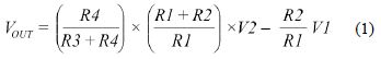
The first suboptimal design is shown in Figure 2. This design is a low-side current sensing application using the OP291. R1 to R4 are discrete 0.5% resistors. According to the formula in the Pallás-Areny article, the best CMR is 64 dB. Fortunately, the common mode voltage is very close to ground, so CMR is not the main source of error in this application. A current sense resistor with a 1% tolerance produces a 1% error, but the initial tolerance can be calibrated or adjusted. However, since the operating range exceeds 80 ° C, the temperature coefficient of the resistor must be considered.
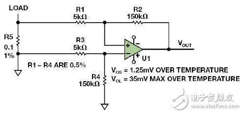
Figure 2. Low-end detection with high noise gain
For very low shunt resistor values, a 4-pin Kelvin sense resistor should be used. Using a high-precision 0.1 Ω resistor and directly connecting the resistor to a one-thousandth of an inch PCB trace can easily increase 10 mΩ, resulting in more than 10% error. But the error is even greater because the copper trace temperature coefficient on the PCB exceeds 3000 ppm.
The shunt resistor value must be carefully chosen. Higher values ​​produce a larger signal. This is a good thing, but the power consumption (I2R) will also increase, possibly as many as a few watts. With smaller values ​​(mΩ level), the parasitic resistance of the line and PCB traces can cause large errors. Kelvin detection is often used to reduce these errors. A special four-terminal resistor (such as the Ohmite LVK series) can be used, or the PCB layout can be optimized to use a standard resistor. If the value is extremely small, PCB traces can be used, but this is not very accurate.
Commercial four-terminal resistors (such as Ohmite or Vishay products) may cost several dollars or more to provide a 0.1% tolerance and a very low temperature coefficient. Performing a complete error budget analysis can show how to improve accuracy with minimal cost increases.
The problem with a large offset (31mV) with no current flowing through the sense resistor is caused by the "rail-to-rail" op amp not swinging all the way to the negative supply rail (ground). The term "rail-to-rail" is misleading: the output will be close to the power rail -- much closer than the output stage of a classic emitter follower -- but never really reach the power rail. The rail-to-rail op amp has a minimum output voltage, VOL, equal to VCE(SAT) or RDS(ON) &TImes; ILOAD. If the offset voltage is equal to 1.25 mV, the noise gain is equal to 30, then the output is equal to: 1.25 mV & TImes; 30 = ± 37.5 mV (due to the VOS, resulting coupled VOL 35 mV). Depending on the polarity of the VOS, the output can be as high as 72.5 mV with no load current. If the VOS maximum is 30μV and the VOL maximum is 8 mV, modern zero-drift amplifiers (such as the AD8539) can reduce the total error to a level mainly caused by the sense resistor.
Another low-end detection application
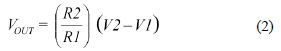
Another example is shown in Figure 3. This example has lower noise gain, but it uses a 3 mV offset, 10-μV/°C offset drift, and a 79 dB CMR low-precision quad op amp. A precision of ±5 mA is required in the range of 0 A to 3.6 A. If ±0.5% sense resistor is used, the required accuracy of ±0.14% cannot be achieved. With a 100 mΩ resistor, a ±5 μmA current can produce a ±500 μV drop. Unfortunately, the offset voltage of an op amp as a function of temperature is ten times greater than the measured value. Even if the VOS is adjusted to zero, a 50°C temperature change will exhaust the full error budget. If the noise gain is 13, then any change in VOS will be expanded by a factor of 13. To improve performance, use a zero-drift op amp (such as the AD8638, ADA4051, or ADA4528), a thin-film resistor array, and a higher-accuracy sense resistor.
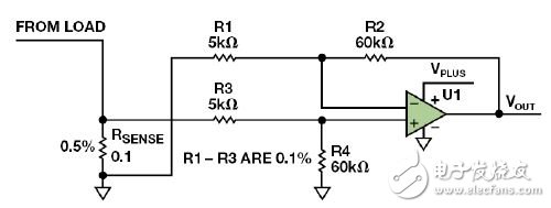
Figure 3. Low-end detection, example 2
High noise gain
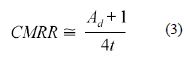
The design in Figure 4 is used to measure the high side current with a noise gain of 250. The OP07C op amp has a VOS maximum rating of 150 μV. The maximum error is 150 μV &TImes; 250 = 37.5 mV. To improve performance, the ADA4638 zero-drift op amp is used. The device has a nominal offset voltage of 12.5 μV over the -40°C to +125°C temperature range. However, due to the high noise gain, the common mode voltage will be very close to the voltage across the sense resistor. The input voltage range (IVR) of the OP07C is 2 V, which means that the input voltage must be at least 2 V lower than the positive rail. For the ADA4638, IVR = 3 V.
Figure 4. High-side current sensing
Single capacitor roll-off
The example in Figure 5 is slightly more complicated. So far, all equations are for resistors; but more accurately, they should take impedance into account. In the case of a capacitor (whether intentionally added or parasitic), the AC CMRR is dependent on the impedance ratio at the target frequency. To roll off the frequency response in this example, add capacitor C2 across the feedback resistor, as would normally be done in an inverting op amp configuration.
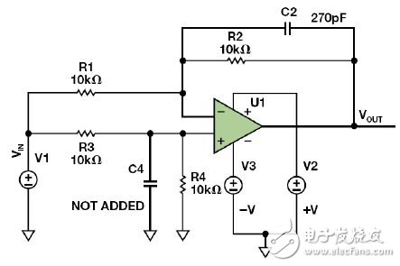
Figure 5. Trying to create a low-pass response
If you want to match the impedance ratio Z1 = Z3 and Z2 = Z4, you must add capacitor C4. It is easy to buy 0.1% or better resistors on the market, but even 0.5% of the capacitors cost more than $1. . Impedance at very low frequencies may not matter, but a difference of 0.5 pF at the input of two op amps due to capacitance tolerance or PCB layout can result in a 6 dB drop in AC CMR at 10 kHz. This is especially important when using a switching regulator.
Single-chip differential amplifiers (such as the AD8271, AD8274, or AD8276) have much better AC CMRR performance because the op amp's two inputs are in a controlled environment on-chip and are typically priced at more than four discrete op amps and four Precision resistors are cheaper.
Capacitance between the inputs of the op amp
To roll-off the differential amplifier's response, some designers will try to add a capacitor C1 between the two op amp inputs to form a differential filter, as shown in Figure 6. This is possible for instrumentation amplifiers, but not for op amps. VOUT will move up and down through R2 to form a closed loop. This does not cause any problems at DC and the behavior of the circuit is consistent with that described in Equation 2. As the frequency increases, the C1 reactance decreases. The feedback into the input of the op amp is reduced, resulting in a gain increase. Eventually, the op amp will operate in an open-loop state because the capacitor shorts the input.
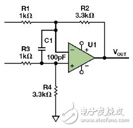
Figure 6. Input Capacitor Reduces High Frequency Feedback
On the Bode plot, the open-loop gain of the op amp drops at -20dB/dec, but the noise gain rises at +20 dB/dec, resulting in a -40dB/dec crossover. As learned in the control system classroom, it must oscillate. In general, never use a capacitor between the inputs of an op amp (except in rare cases, but this article does not discuss it).
in conclusion
Whether it is discrete or single-chip, the four-resistor differential amplifier is widely used. In order to obtain a stable and worthwhile production design, the noise gain, input voltage range, impedance ratio, and offset voltage specifications should be carefully considered.
Outdoor Trolley Power Supply,Solar Energy Storage,Outdoor Charging Station,Outdoor Storage Battery
Sichuan Liwang New Energy Technology Co. , https://www.liwangnewenergy.com