1 Introduction
This article refers to the address: http://
Video image acquisition is the front-end part of the video signal processing system and is developing in the direction of high speed, high resolution, high integration and high reliability. Image acquisition system has a wide range of applications in industrial, military, and medical fields, such as remote monitoring, security, remote meter reading, video telephony, industrial control, image pattern recognition, and medical devices. Application [1]. This paper introduces an FPGA-based image acquisition system, users can reconfigure the logic modules and I/O modules inside the FPGA as needed to achieve system reconstruction [1] [2]; and adopt this design scheme, Facilitate the timely detection of errors in the design, which can effectively shorten the development time and improve work efficiency.
2. The overall framework and working principle of the system
The whole system is mainly divided into four modules: video decoding module, video encoding module, memory module and FPGA core control module. The overall framework of the system is shown in Figure 1.
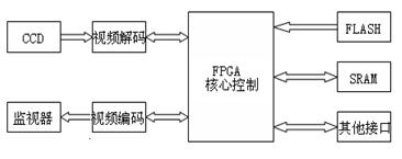
Figure 1 Overall block diagram of the system
The main functions of the FPGA implementation are: initialization of the video codec device, acquisition and storage of the video image, and sending the captured image data to the monitor through the video encoding chip.
The working principle of the system is: after the system is powered on, the FPGA completes the video decoding and initialization of the encoding chip through the program in the FLASH; after receiving the interrupt signal of the video AD conversion, the FPGA transfers the converted digital image data to the SRAM to save After one frame of image conversion is completed, the FPGA transfers the digital image in the SRAM to the video encoding chip for display on the monitor, and starts to control the acquisition of the next frame image.
3, hardware circuit design
3.1 AD and DA conversion module
The video codec chips used in this system are ADV7181 and ADV7177. The hardware circuit design of AD and DA conversion devices are introduced below.
3.1.1 AD Conversion Module
ADV7181 system is a video decoder chip [3] introduced by AD company. It has the following features: I2C bus interface, 6 channels of analog video input, support NTSC, PAL, SECAM video system, support multiple analog input formats and multiple numbers Output format.
In this system, channel 1 is selected as the PAL CVBS video input, and the data output can be output in 8-bit or 16-bit format as needed. The interface circuit of ADV7181 and FPGA is shown as in Fig. 2.
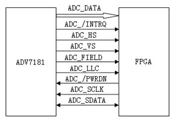
Figure 2 ADV7181 and FPGA interface circuit
After the system is powered on, the initialization configuration of the ADV7181 is completed through the I2C module of the FPGA, where ADC_SCLK and ADC_SDATA are the clock lines and data lines of the I2C bus, respectively. ADV7181 outputs horizontal sync signal ADV_HS, vertical sync signal ADV_VS, field sync signal ADV_FIELD, interrupt signal ADC_/INTRQ, ADC_LLC sync signal and image data signal ADC_DATA (8-bit or 16-bit configurable output), and ADC_/PWRDN, respectively. The signal controls whether the ADV7181 is operating in power save mode. Users can select horizontal, vertical and field sync signals (CCIR-601 format) or ADC¬_LLC signals (CCIR-656 format) to synchronize the system and video input, and use these synchronization signals to control the converted video data. Write memory operations.
3.1.2 DA Conversion Module
DA conversion adopts ADV7177[4] of AD company, which has the following characteristics: I2C interface, 3 channels of analog video output, support for multiple digital input formats and various analog output formats, users can choose to use according to needs. Its circuit design is similar to that of ADV7181. The interface circuit of ADV7177 and FPGA is shown as in Fig. 3.
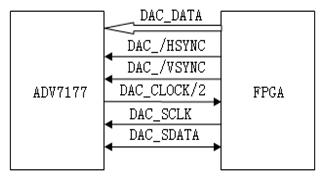
Figure 3 ADV7177 and FPGA interface circuit
DAC_DATA is the input digital video signal, DAC_/HSYNC, DAC_/VSYNC are the horizontal and vertical sync signals, DAC_CLOCK2 is the 27M or 13.5M synchronous clock of the ADV7177 output (related to the configuration data of the register), DAC_SCLK, DAC_SDATA is the I2C of the ADV7177 Configure the bus.
3.2 FPGA core control module
The FPGA core control module uses ALTERA's Cyclone II series of EP2C20[5], which has a high cost performance: EP2C20 has up to 315 user pins, four PLLs, 26 embedded 18*18 multipliers, and 52 M4K RAM block, 186,752 logic cells; divided into 8 I/O banks, each bank can be configured with 1.2V or 3.3V I/O level as needed to facilitate connection with peripheral circuits. Taking into account the actual needs of the system, the EP2C20Q240 with a 240-pin PQFP package is used in the system.
In this system, the FPGA mainly completes the initial configuration of the video AD and DA and the read/write control of the memory. It completes the acquisition of the video data through the interrupt signal of the AD, and puts the collected data into the storage module. After one frame, the data is transferred to the video encoding chip and displayed on the monitor while starting to acquire the next frame image.
In this system, the FPGA adopts two configuration modes: JTAG and AS. For specific design, please refer to ALTERA data sheet [5].
3.3 Memory and other modules
Due to the limited RAM resources inside the FPGA chip, it is impossible to store too much video data and process it. Therefore, in this system design, two SRAM chips are added to assist the FPGA in video signal acquisition. Two SRAMs can be used for 16-bit data storage, so the ADV7181 and ADV7177 can be configured to operate in 8-bit or 16-bit data as needed, increasing system flexibility.
The SRAM chip used in the design of this system is IDT71V424[6] produced by IDT Company of USA. It is a high-speed static memory produced by high-performance and reliable CMOS technology. Its single-chip storage capacity is 512K*8Bit, with high-speed access. Time, 10 or 12 ns. The internal part is completely composed of a static asynchronous circuit, and it is possible to directly cover the useless data without inputting a clock signal or refreshing the chip.
In order to ensure the effectiveness of the control signal in the actual design, the three control lines SRAM_/WE, SRAM_/OE, SRAM_/CS are respectively connected to the FPGA chip by adding a 4.7K pull-up resistor. The specific circuit is shown in Figure 4:
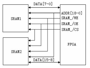
Figure 4 SRAM and FPGA interface circuit
In addition, in order to reduce the mutual interference between the analog and digital systems, the power module uses a digital power supply and an analog power supply to design the last point of the common design. Mainly used TI's TPS54612, TPS64616 to provide FPGA 1.2V core voltage and 3.3V IO voltage respectively; analog 1.8V and 3.3V use AMS1117 series power chip.
4, system software design
This system software was developed in the Quartus II environment using the Verilog language. Mainly include: 1, initial configuration of AD and DA chips, 2, video image acquisition, 3, video image storage and DA conversion.
4.1 I2C Configuration Module
After the system is powered on, the AD and DA chips are reset respectively, so they need to be initialized. The program stores the initial value of the register in an array in advance. When the control register is set, the FPGA writes the data in the order of the configuration address, control register address, and register value of the AD or DA through the I2C bus, and initializes the AD and DA. The flow of the I2C configuration module [7] [8] is shown in Figure 5.
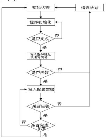
Figure 5 Flow chart of I2C configuration
4.2 Video image acquisition module
In this system, the ADV7181 chip outputs 8 bits in CCIR-656 format (can also be configured as 16-bit output as needed), and its effective resolution is 720*576, interlaced. The digital video data format it outputs is shown in Table 1.
Table 1 Digital Video Format Table of ADV7181 Output

In the actual logic design, the main task is to discriminate and detect the line start flag code and the line end flag code of the CCIR-656 format. The specific design is as follows: Under the synchronous control of the 27MHz pixel clock signal ADC_LLC, the 8-bit digital video data is continuously input into the FPGA chip by the ADV7181 chip, and the FPGA first detects the three bytes "FF 00 00" for these three The detection of bytes only needs to be designed with a simple finite state machine. After detecting the above three bytes, the FPGA then detects the unknown byte immediately following the three bytes. If the value of the 4th bit of the unknown byte is 0, it is SAV byte, if it is 1 , it means it is an EAV byte. Table 2 shows the data formats of SAV and EAV.
Table 2 Data format table of SAV and EAV

With the above analysis, the acquisition process [7] [8] of the effective video data shown in Fig. 6 can be obtained.
In this paper, the image acquisition program is designed according to the above process. Figure 7 is the waveform of the acquired image data obtained by using the logic analyzer tool provided by Quartus II. The sampling clock of the logic analyzer is 27M ADC_LLC signal, and data_in is image data. Ad_hs is a horizontal sync signal.
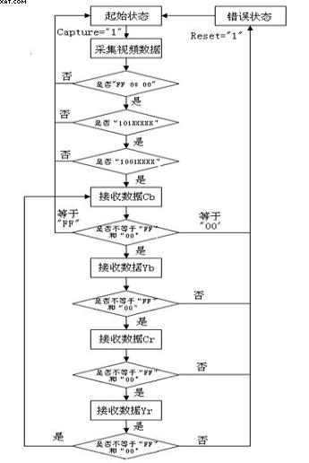
Figure 6 Collection process of effective video
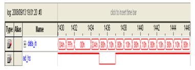
Figure 7 Image data signal obtained by FPGA acquisition
4.3 Video Image Storage Module and DA Conversion Module
Due to the limited RAM resources in the FPGA, and for the future expansion, the system adds two pieces of video data collected by the 512K*8 SRAM memory buffer. After one frame of image acquisition is completed, the FPGA writes the data in the SRAM to the DA conversion chip, and starts the acquisition of the next frame. In this system, the video encoding chip receives the standard 8-bit CCIR-656 data, and the output is a CVBS composite video signal. The initial configuration and working process of the ADV7177 is similar to that of the ADV7181 and will not be described here.
5, the experimental results
According to the above design scheme, the hardware design and software debugging of the system are completed. Figure 8 shows a video image displayed on the monitor collected by the system. The ADV7181 adopts the 8-bit CCIR-656 output format and the output format of the ADV7177. For CVBS video signals.
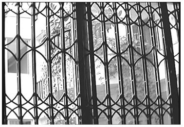
Figure 8 A video image captured by the system
6 Conclusion
The experimental results show that the system works stably and reliably, and can meet the requirements of high performance real-time image processing system. In addition, the system adopts FPGA design scheme, with high integration and flexible design, and users can perform system reconstruction according to their own needs, which is convenient and fast, and has high application value.
Cross of cable tray is an essential component of cable tray systems used in various industries. Cable trays are used to support and protect cables and wires in buildings, factories, and other infrastructure projects. The cross of cable tray is a junction that connects two or more cable trays to create a network of cable management.
The cross of cable tray is designed to provide a secure and stable connection between cable trays. It is usually made of steel or aluminum and is available in different sizes and shapes to accommodate various cable tray configurations. The most common shapes of the cross of cable tray are T-shaped, X-shaped, and Y-shaped.
One of the main benefits of using a cross of cable tray is its flexibility. It allows for easy expansion and modification of the cable tray system without the need for additional support structures. This makes it an ideal solution for projects that require frequent changes to the cable layout.
Another advantage of the cross of cable tray is its durability. It is designed to withstand harsh environments and extreme temperatures, making it suitable for use in industries such as oil and gas, mining, and chemical processing. It is also resistant to corrosion, which ensures a longer lifespan and reduces maintenance costs.
Cross Of Cable Tray,Tee Cross Cable Tray,Elbow Cross Cable Tray,Cross Cable Tray
Rayhot Technology Group Co.,Ltd , https://www.cnrayhot.com
