Fan-out packaging is a mature technology used in many mobile applications. The early semiconductor packaging has always been single-chip packaging. To support the development trend of increasing wiring density due to increased functions, more complex packaging, stacked packages, and systems inpackages are required. high performance. With the development of technology, fan-out packaging is reducing the contradiction between cost and high performance. Whether it is to make the wafer thinner to meet the needs of smaller size, and to save the cost of solder, or as a process platform for the first process of redistribution-layer (RDL), all packages require temporary bonding (temporary bonding). ).
Temporary bonding requires two processes: bonding and debonding. From fan-out wafer-level packaging (FoWLP) to power devices, each application has unique requirements in terms of process temperature, mechanical stress, and thermal budget, so determine the appropriate lift-off technology comparison difficult. Here are just a few examples, the actual situation is more complicated. In this article, we will focus on laser debonding: For example, what conditions can be applied to materials that are more compatible with high temperature resistance, and which applications are suitable for the characteristics of laser debonding.
In order to control the heat input caused by peeling, UV lasers are often used to peel off different temporary bonding materials provided by different material suppliers. In order to ensure the lowest maintenance workload, diode-pumped solid-state (DPSS) can combine highly process-controlled beam-shaping opTIcs with the lowest heat input, which is correct. s Choice.
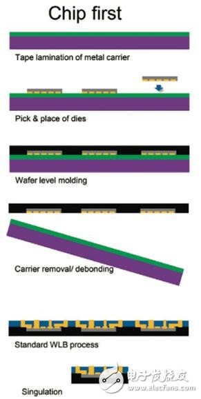
Figure 1 Schematic diagram of the manufacturing process of Chipfirst fan-out wafer-level packaging
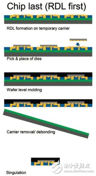
Figure 2 Schematic diagram of the manufacturing process of Chiplast fan-out wafer-level packaging (also known as RDL first)
Challenges of Temporary Bonding in Fan-Out Wafer Level Packaging (FoWLP)
FoWLP can reap huge benefits in the industry, to a certain extent, depends on its use of carrier, and temporary bonding materials have high requirements for chemical and thermal compatibility. Certain polyimides meet this harsh environment and are also suitable for laser lift-off.
Although bonding and stripping are both FoWLP processes, the requirements of the two are very different. By observing the different semiconductor processes in various applications, it is clear that no one lift-off process solution is compatible with all semiconductor processes, and multiple solutions are an inevitable choice. This is why the various stripping processes developed (the stripping technology is a feature of temporary bonding) are still in use today.
Comparison of mainstream stripping techniques
The most common methods are: thermal slide-off debonding, mechanical debonding and UV laser debonding. These three methods are all suitable for mass production, with huge differences in process compatibility.
Thermal slide-off debonding (thermal slide-off debonding) is a method that uses thermoplastic materials as an adhesive interlayer between the device and the carrier wafer. This method takes advantage of the reversible thermal properties of thermoplastic materials, which means that at higher temperatures, the viscosity of the material will decrease, so that peeling can be accomplished by simply sliding the wafers on both sides. The feature of thermal peeling is based on the temperature characteristics of the thermoplastic material, the use range is between 130°C and 350°C, so bonding and peeling can be completed at a higher temperature. Temperature stability depends to a large extent on mechanical stress, which we can observe is due to the low viscosity of thermoplastic materials at high temperatures.
Mechanical debonding is a method that highly depends on the characteristics of the wafer surface, the adhesion and cohesion of the temporary bonding material. For most material systems, a mechanical release layer can be used to achieve controlled release. The main feature of mechanical peeling is that it can be processed at room temperature and strongly relies on mechanical stress. Since mechanical peeling requires low adhesion between the temporary bonding material and the wafer to be successfully peeled; therefore, it is somewhat difficult to use this method in FoWLP applications. This is because the higher stress generated in the FoWLP process will cause spontaneous peeling, even in the thinning process, which will lead to a sharp decline in yield.
Laser debonding is a technique that uses several different variables to achieve debonding. The peeling mechanism of this method depends on the type of laser, temporary bonding glue, and the specific release layer used in the process. Infrared laser lift-off relies on a thermal process to work: it absorbs light and converts it into heat, thereby generating high temperatures in the bonding interface. UV laser lift-off usually relies on a chemical process to work: the energy absorbed by light is used to break chemical bonds. Breaking the chemical bonds of the polymer will cause the original polymer to decompose. The decomposition products include gas, which will increase the pressure of the bonding interface and thus help peeling. Since the temporary bonding glue has high adhesion to the wafer before the stripping process, this method is very suitable for FoWLP applications.
Optimized solution for fan-out wafer level packaging (FoWLP) applications
According to Memes Consulting, due to the limited heat input during the stripping process, UV lasers have more advantages in FoWLP. The carrier wafer must be able to pass through the ultraviolet laser to ensure effective use of laser energy and extend the life of the carrier wafer. There are currently two main types of ultraviolet lasers (all-solid-state lasers and excimer lasers), each of which can be selected from multiple wavelengths. A laser with a wavelength greater than 300nm is the most ideal choice for the following two reasons: first, the laser lift-off material available in the market can effectively absorb and lift lasers with a wavelength higher than 300nm; secondly, because glass can be used in this High transmission is achieved within the band, that is, the laser in this band allows the use of standard glass wafers as the carrier.
Since the all-solid-state laser does not require periodic replacement of halogen gas, the maintenance cost is low. And the power consumption is very low. Calculated based on the power consumption of working 7 days a week and working 24 hours a day, the all-solid-state laser can run for 5 years. In addition, since the optical arrangement is compact, it is advantageous to realize a smaller size pin. Figure 3 shows the Gaussian beam common to all solid-state lasers.
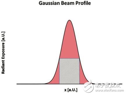
Figure 3 Generally all solid-state lasers require high pulse overlap. The overlapping area represents the radiant exposure used in laser lift-off, while the red area represents the energy that cannot be used for lift-off
UV laser peeling has a threshold requirement for radiation energy, which means that peeling occurs above a certain value of radiation exposure. In Fig. 3, the overlapping area indicates that the radiation exposure is suitable for peeling. Energy below or above this value (the red area in the figure) cannot be stripped, and is usually converted into heat energy, which will cause carbonization and particle generation. Since the laser beam at the edge of the Gaussian distribution lacks sufficient energy, there must be a certain pulse overlap. At this time, additional variable optimization is necessary to successfully peel off without carbonization. In addition, excess energy in the center of the beam can cause carbonization. The Gaussian beam is not suitable for limiting the thermal effect in peeling.
By using a dedicated optical device for beam shaping, the Gaussian beam can be shaped into a near top hat beam. By using this optical device, a beam with good reproducibility for stripping can be obtained, and the shape is similar to the top hat beam in Figure 4 (on this basis, the shape of the beam will not change with time), thereby limiting the heat input . Combined with the high pulse repetition rate of this laser, stricter process control can be achieved, and the surface of the fixed wafer can be scanned, thereby achieving high output in the lift-off process. Figure 5 depicts the scanning process. Compared with the excimer laser, the wafer is fixed on a stationary stage, and the laser spot is controlled by a galvo scanner above the wafer. The entire stripping process is faster and can achieve high output.
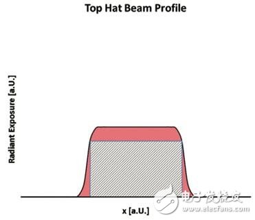
Figure 4 An advanced UV laser solution that uses beam shaping optics to combine high repeatability scanning with laser energy efficiency. In the overlapping area, the radiation irradiation efficiency for peeling is very high
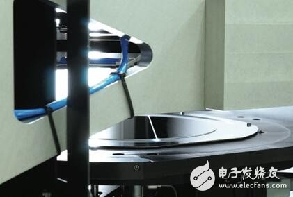
Figure 5 The EVG laser lift-off solution combines an all-solid-state laser with beam shaping optics to achieve a controllable process with high output
As shown in Figure 6, the test wafer was used to determine the optimal radiation exposure value for peeling. Even for top hat beams, in order to reduce thermal effects, it is very important that the radiation exposure value is close to the peeling threshold. Nevertheless, less overlap is necessary because the adhesion between the temporary bonding material and the wafer is very high.
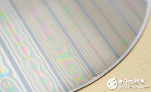
Figure 6 Test wafer used for laser lift-off, different tracks represent the lift-off effect of different lasers
Temporary bonding of future fan-out wafer level packaging (FoWLP)
Ultra-thin fan-out stacked package (FoWLP), also known as package on package (PoP), has been included in the technology roadmap for many applications because this type of package can greatly increase device density. However, in the future, PoP will require thinner thickness for reconstituting wafers (reconsTItuted wafers), which will bring more challenges to temporary bonding. For example, the bow of temporarily bonded wafers composed of a stack of molded wafers and carrier wafers must be minimized to ensure uniform thinning. The maximum total thickness variation (TTV) specification will also become stricter based on the thickness of the final wafer. For different 3D applications, problems related to connection, such as choosing "via first" or "via last", have also become more in PoP. Although there are multiple processes to choose from, no fan-out packaging company has a standard process flow.
to sum up
Since the UV laser can be stripped at room temperature and chemically stable materials can be used, the UV laser stripping is a kind of suitable for both chip first and chip last (or RDL-first) fan-out wafer-level packaging (FoWLP) method. The UV laser lift-off solution introduced in this article not only combines the advantages of all solid-state lasers, but also has the advantages of low maintenance cost and low power consumption. Thanks to the special beam shaping optics, it also realizes the combination of high pulse frequency and high space control.
53 Jack.We are manufacturer of 6p6c Female Connector in China, if you want to buy RJ11 Jack Full Plastic MINI,6 Pin RJ11 Modular Connector,RJ11 Jack Full Shielded please contact us.
The RJ-45 interface can be used to connect the RJ-45 connector. It is suitable for the network constructed by twisted pair. This port is the most common port, which is generally provided by Ethernet hub. The number of hubs we usually talk about is the number of RJ-45 ports. The RJ-45 port of the hub can be directly connected to terminal devices such as computers and network printers, and can also be connected with other hub equipment and routers such as switches and hubs.
6p6c Female Connector,RJ11 Jack Full Plastic MINI,6 Pin RJ11 Modular Connector,RJ11 Jack Full Shielded
ShenZhen Antenk Electronics Co,Ltd , https://www.pcbsocket.com
