Pin assignment is a very important part of FPGA hardware design, especially on hardware circuits that require pins that are compatible with other chips. The state of the pins of each stage of the Xilinx FPGA from power-on to normal operation has a very important impact on hardware design and pin assignment. This topic is aimed at analyzing the state of all IOs from FPGA power-on, configuration procedures, to normal operation.
From the time phase can be divided into two parts, the first phase is from the FPGA power-on until the configuration (ConfiguraTIon) is completed. The second phase begins after the configuration is complete and the FPGA begins normal operation.
From the pin type, it can be divided into three categories: The first type is ordinary IO, which is divided into IO used in programming and IO not used in programming (that is, there is no ucf or XDC file). The constrained IO); the second type is dedicated download configuration pins (Dedicated Pins), these pins are only used for dedicated functions, including M[2:0], TCK, TMS, PROGRAM_B, INIT_B, etc. The third type is function-multiplexed pins. These pins are used when certain functions are used. For example, when using the BPI configuration mode, D[00-31] and A[00-28] are required. If SYSMON is used, I2C_SDA and I2C_SCL need to be used. However, in the case where this function is not currently used, the function multiplex pin can be regarded as a normal IO.
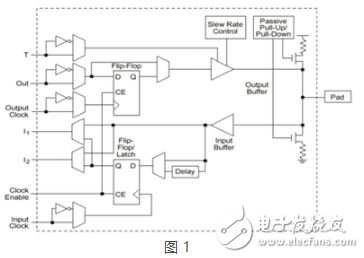
The basic structure of FPGA IOIn the "IO input and output modes" introduced the various input and output modes and principles of the processor IO, then what is the structure and principle of the FPGA IO? Figure 1 shows the internal structure of the IOB provided in the Xilinx documentation. It can be seen that:
Inside the FPGA IOB, a pull-down resistor is built in before the Pad output. The Passive Pull-up/Pull-down module can be used to control whether the two MOS transistors are turned on or off to control whether the pull-up resistor is enabled.
The internal connection Pad has an Input Buffer and an Output Buffer respectively. The Input Buffer should always be in a high-impedance state, and the level on the Pad can be passed to the I1 and I2 through the Input Buffer, or the lower FF. The Output Buffer has two control signals, Slew Rate Control, which is used to control the Slew Rate of the output signal. The other is the three-state control signal T, which controls the output Buffer output high impedance.
The internal output signal Out can be output through the upper half of the FF, synchronized by the Output Clock, or directly connected to the input of the Output buffer.
The output of the same Input Buffer can be directly connected to I1 and I2, or it can be output to the internal bus after synchronization of the input clock through the FF of the lower half.
The upper and lower MOS are not the two MOS transistors of the push-pull output, because they are not controlled by the complementary signal, and not necessarily one is turned on and the other is closed.

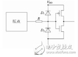
Here is a description of the structure and principle of the input buffer. Its structure is shown in Figure 2. The principle is very similar to the push-pull output circuit, except that the input signal acts as the control end of two complementary MOS transistors, controlling the level of the output. . Since the input buffer has its own supply voltage, the input level must match the supply voltage of the buffer. Two clamp diodes, D1 and D2, are used to prevent the input voltage from being too low or too high, damaging the input buffer.

Before configuration is complete
Before the FPGA is powered up to the configuration, since the current FPGA has not yet downloaded the program, it is impossible to distinguish which pins are used by the design and which pins are not used. The normal IO at this time consists of two parts:
1. All general purpose IO pins in this package.
2. All function multiplexed pins that are not used in the currently selected mode.
The state of these pins in the Spartan6 family and previous devices is determined by the state of the HSWAPEN.

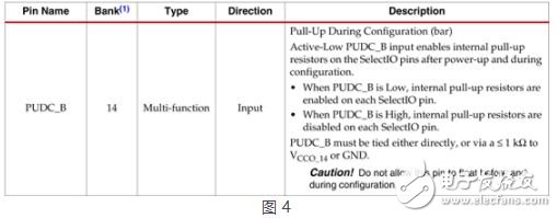
In devices after the 7 series, including Ultrascale devices, the state of these pins is based on the PUDC_B (Pull-Up During ConfiguraTIon) pin.

The functions of these two pins are similar and are used to control whether all normal IO pull-up resistors are enabled before ConfiguraTIon is completed. Corresponding to Figure 1, the Output Buffer output is high impedance, and the Input Buffer is always high impedance. In this case, select whether to connect the pull-up resistor.
After the configuration is complete
After the configuration is complete, the FPGA enters the normal working mode. After the configuration is completed, the common pins can be divided into the following two types:
The IO used in engineering design, that is, the IO that is clearly constrained in UCF or XDC.
The rest are not used, nor are there any constraints on IO. (called Unassigned Pins)
First, for the first case, since the settings of these pins have been explicitly set in the design, including direction, level, drive capability, etc., after the configuration is completed, the status of these pins has been set to pre- Set the status.
The sensor includes linear encoder and rotary encoder, which is used for the position measurement of speed, displacement and angle. Yuheng optics can provide rotary encoders based on optical, magnetic and gear principles, linear encoders based on optical principles and supporting products.

Custom Sensor,Clintegrity Encoder,Absolute Angle Encoder,Small Rotary Encoders
Yuheng Optics Co., Ltd.(Changchun) , https://www.yuhengcoder.com
