First, Buck switch regulator :
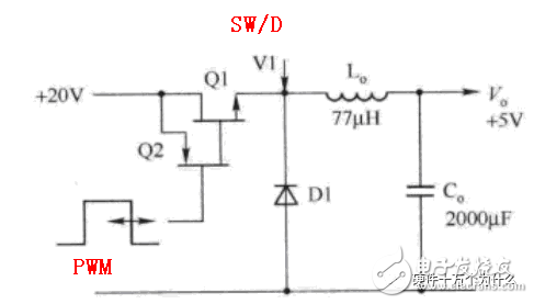
Second, CCM and DCM definition:
1 , CCM (ContinuousConduction Mode), continuous conduction mode: the inductor current never goes to 0 during one switching cycle . Or the inductor is never "reset", meaning that the inductor flux never returns to zero during the switching cycle , and there is current flowing through the coil when the power tube is closed.
2 , DCM , (Discontinuous Conduction Mode) discontinuous conduction mode: In the switching cycle, the inductor current will always reach 0 , which means that the inductor is properly "reset", that is, when the power switch is closed, the inductor current is zero.
3 , BCM ( Boundary Conduction Mode ), boundary or boundary line conduction mode: The controller monitors the inductor current. Once the current is detected to be equal to 0 , the power switch is immediately closed. The controller always waits for the inductor current to "reset" to activate the switch. If the inductor value current is high and the ramp is fairly flat, the switching period is extended, so the BCM variator is a variable frequency system. The BCM converter can be referred to as a critical conduction mode or a CRM ( Critical Conduction Mode ).
Figure 1 shows three different modes of operation by the flower inductor current curve.
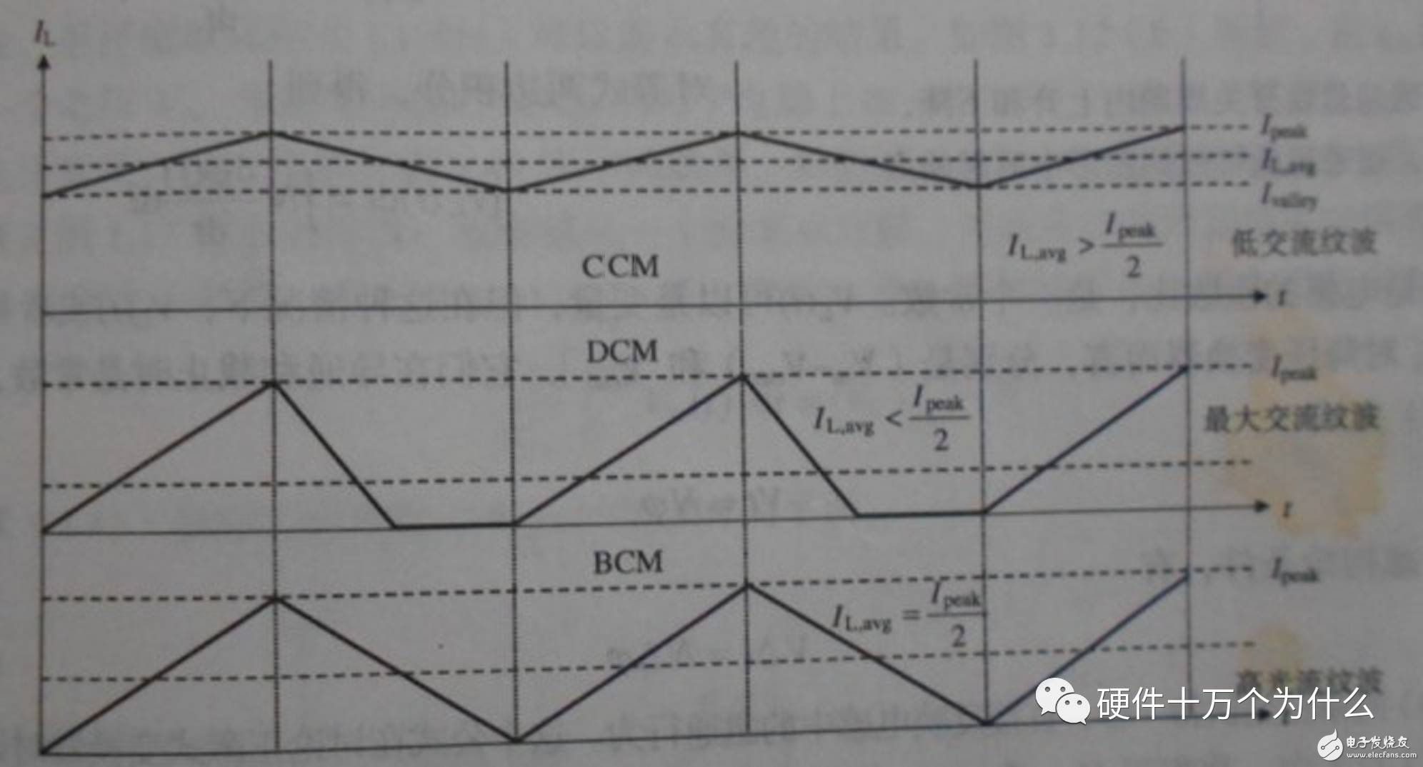
Figure 2 Three modes of inductor operation: CCM, DCM, BCM
The midpoint amplitude of the current ramp is equal to the DC output current  Average value
  With valley current
  The difference is the ripple current .
Third, CCM working mode and characteristics
According to the CCM definition, the waveform of the buck converter operating in continuous mode is tested, as shown in Figure 3 below.
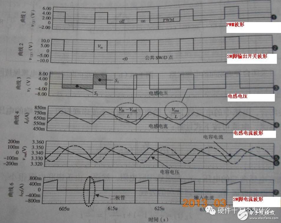
image 3
Waveform 1 represents the PWM pattern, which triggers the switch to turn on and off. When the switch SW is turned on, the voltage at the common point SW/D is Vin . Conversely, when the switch is turned off, the common point SW/D voltage will swing to negative, at which point the inductor current provides a bias current to diode D , which exhibits a negative buck-freewheeling action.
Waveform 3 describes the change in voltage across the inductor. At the equilibrium point, the average voltage across the inductor L is zero , and S1 + S2 = 0 . The S1 area corresponds to the product of voltage and time when the switch is turned on, and the S2 area corresponds to the product of voltage and time when the switch is turned off. S1 simply uses a rectangular height  Multiply by
  And S2 is also rectangular height -
  Multiply t ( 1-D )
  .
.

Can be seen from the above formula  It varies with D ( duty cycle ) . Ideally, the transfer characteristics are independent of the output load. However, the book says that this description is not very accurate. I will tell you carefully after I have read it carefully.
In fact, let's look at the last waveform above. When the switch is closed, the SW/D point current waveform has a big spike. I have measured the voltage waveform myself. I use the voltage chip ACT4065 and ACT4065A, as shown in Figure 4 . 5 , the specific reasons are as follows.
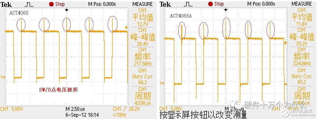
Figure 4 Figure 5
First, because the switch is closed, it will  Acting on the cathode of the diode suddenly interrupts the conduction period of the diode. For PN diode, a PN junction is first necessary to return to electrically neutral PN junction becomes forward conduction when the time to remove all of the minority carriers. It takes a certain amount of time for the diode to remove all of the injected charge to return to its off state, which exhibits a short circuit behavior before it is fully recovered. For Schottky diodes, there is a metal-semiconductor silicon junction that has no recovery effect, however, it has a large parasitic capacitance and a junction capacitance . When the diode is turned on, once discharged, the SW quickly passes through the discharge capacitor.
  , produces a current spike. So slowing down the switch SW time will help reduce the spike current.
Second, it is related to the shape of the current. It can be seen from the image that the output ripple (capacitor current waveform) is small. The output ripple is smooth and "no pulse". This means that the output current signal is well accepted by subsequent circuits, ie less pollution in the power supply. In addition, the input current not only has spikes, but also looks like a square wave. If the value of the inductance L tends to infinity, the waveform of the input current is a real square wave. Therefore, this current is a "pulsating" current, containing a large amount of contamination, which is more difficult to filter than a typical sinusoidal current.
Square wave : consists of odd harmonics of a sine wave , that is, consisting of sinusoidal frequencies 1, 3, 5, 7...n .
There are also spikes at the moment when the switch is turned off. I think it should be related to the parasitic capacitance and junction capacitance of the diode and SW pin.
Through the above , the characteristics of the CCM step-down variator can be summarized :
1, D is limited to less than 1 , the output voltage of the buck converter is always less than the input voltage;
2. If the various ohmic losses are ignored, the transform coefficient M is independent of the load current;
3. By changing the duty cycle D , the output voltage can be controlled;
4. The buck converter works in CCM and will bring additional losses. Since the freewheeling diode reverses the charge recovery time takes time to consume, which is an additional loss burden for the power switch tube;
5. The output has no pulse ripple , but there is a pulse input current.
Fourth, DCM work mode and related features
The switching device operates in CCM mode when the load current is large , but when the load current decreases, the ripple current will decrease as a whole, as shown in Figure 2 , when the load current decreases to half of the peak-to-peak value of the harmonics,

, The lowest point of the ramp just down to zero, at the lowest point, the inductor current is zero, zero inductive energy storage. If the inductive load current is further reduced, the inductor will enter the DCM mode of operation, and the voltage and current waveforms will vary greatly as shown in Figure 6 , and the transfer function will vary greatly.
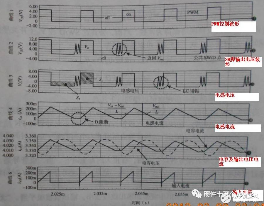
Figure 6
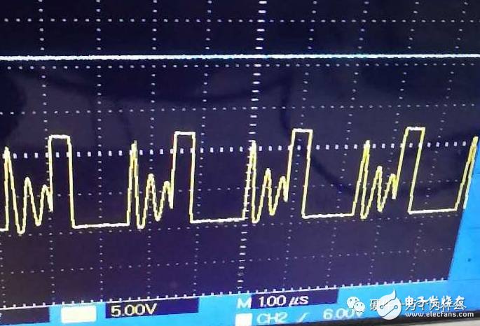
From waveform 4 , it can be seen that the inductor current drops to zero , causing the freewheeling diode to turn off. If this happens, the left end of the inductor is open. In theory, the voltage at the left end of the inductor should return , because the inductor L no longer has current and does not oscillate. However, due to the existence of many parasitic capacitances around it, such as the parasitic capacitance of the diode and SW , an oscillating circuit is formed. Like curve 2 and curve 3 , a sinusoidal signal appears and disappears after several cycles, which is related to resistance damping. However, there may be differences in the actual test. For example, in the ACT4065A test, the SW/D waveform is tested , but the oscillation is in the middle, as shown in Figure 7 , the supplier engineer said that this is in DCM mode, but I did not find it. Relevant information for verification.
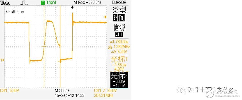
Figure 7
The Buck transformer controls the output voltage to a constant value over the entire load range, even if the inductor enters a discontinuous mode of operation. Therefore, it is easy for us to misunderstand that the inductor enters the discontinuous mode of operation and has no effect on the circuit operation. In fact, the transfer function of the entire circuit has changed and the control loop must adapt to this change.
For the Buck regulator, there is nothing wrong with the inductor entering a discontinuous mode of operation. DC output voltage before entering discontinuous mode

Note that this formula is independent of the load current parameter, so when the load changes, the duty cycle D does not need to be adjusted and the output voltage remains constant. In fact, when the output current changes, the on-time will also change slightly, because the turn-on voltage drop and inductance of Q1 change slightly with the change of current, which requires Ton to make appropriate adjustments.
After entering the DCM operation, the transfer function will change, the transfer function of the CCM will no longer be applicable, and the on-time of the switch will decrease as the DC output current decreases. The following is the transfer function in the DCM mode of operation, the duty cycle is related to the load current, ie

Because the control loop is to control the output voltage to be constant, the load resistance R is inversely proportional to the load current. Assuming Vout , Vin , L , T , and constant, in order to control the voltage constant, the duty cycle must vary with the load current.
At the critical transition current, the transfer function transitions from CCM to DCM . When operating CCM , the duty cycle remains constant and does not change with load current; when operating at DCM , the duty cycle changes as the load current decreases.
Through the above , the characteristics of the DCM buck converter can be summarized :
1, M depends on the load current;
2. For the duty cycle of the figure, the transfer coefficient M under DCM is larger than the CCM. The load current is low and the depth is DCM, and M is easy to reach 1 .
Five, Buck regulator inductance selection:
In order to reduce the critical output load current when entering the discontinuous mode, we can reduce the critical output load current by increasing the inductance L. The circuit operates in continuous mode over the desired load current range.


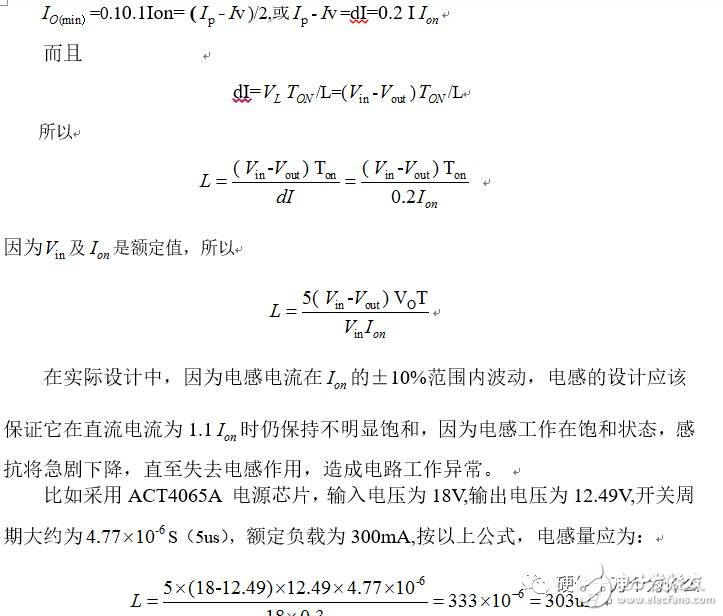
According to the theoretical calculation, we should use 303uH, but in practice we only use 68uH, part of which is related to cost, and also related to the characteristics of my product itself, the space is small, if the large inductance can not be put down at all, in fact, personally feel that it is enough.
The following are some of the waveforms for the output load current threshold as a function of inductance when testing the ACT4065A :
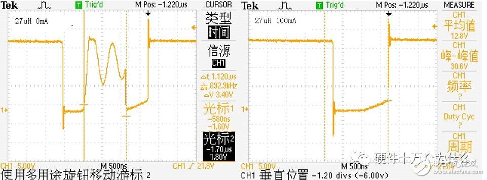
1 ), L1=27uH, Uo=12.51V
By changing the magnitude of the load current and observing the output waveform, the oscillation waveform width is reduced when the load current is gradually increased at L1=27uH . When the waveform reaches 100mA , no waveform is generated when the waveform is turned off, and the normal switching state is reached.
0mA 100mA
2 ), L1=33uH, Uo=12.51V
  By changing the magnitude of the load current and observing the output waveform, the oscillation waveform width is reduced when the load current is gradually increased at L1=33uH . When the waveform reaches 55mA , no waveform is generated when the waveform is turned off, and the normal switching state is reached.
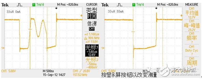
0mA 55mA
3 ), L1=47uH, Uo=12.51V
  By changing the magnitude of the load current, observe the output waveform. When L1=47uH , the oscillation waveform width decreases when the load current gradually increases. When the voltage reaches 45mA , no waveform is generated when the waveform is turned off, and the normal switching state is reached.
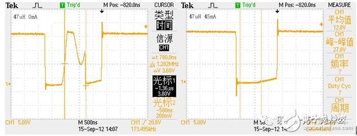
0mA 47mA
4 ), L1=68uH, Uo=12.51V
  By varying the size of the load current, the output waveform is observed, at L1 = 68uH, the load current is gradually reduced to increase the degree of oscillation waveform, is reached 30mA, the waveform without oscillation waveform is generated at turn-off, to achieve a normal switching state.
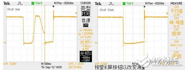
0mA 30mA
5 ), L1=136uH, Uo=12.51V
  By changing the magnitude of the load current, observe the output waveform. When L1=136uH , the oscillation waveform width decreases when the load current gradually increases. When the voltage reaches 20mA , no waveform is generated when the waveform is turned off, and the normal switching state is reached.
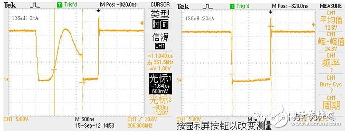
0mA 20mA
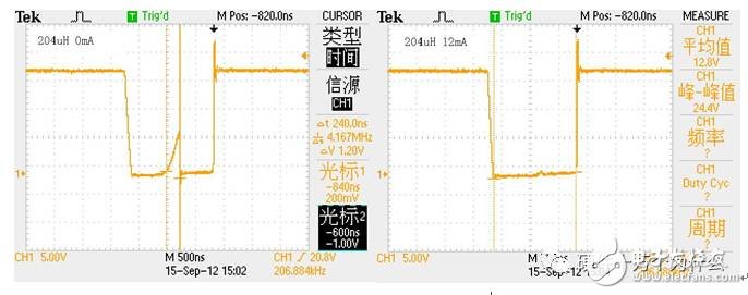
6 ), L1=204uH, Uo=12.51V
  By changing the magnitude of the load current, observe the output waveform. When L1=204uH , the oscillation waveform width decreases when the load current gradually increases. When the voltage reaches 12mA , no waveform is generated when the waveform is turned off, and the normal switching state is reached.
0mA 12mA
Based on the above and test waveforms, for the ACT4065A chip , when the inductance is gradually increased and the SW is turned off, the oscillation waveform width is reduced; the larger the inductance, the smaller the load current can be used to eliminate the oscillation waveform. , but this is the case within 10mA .
5. Comparison of CCM and DCM :
. 1, DCM is a terrific feature, it can reduce power consumption, some of the DCM higher conversion efficiency, energy belonging fully converted;
2 , working in DCM mode, the output current ripple is larger than CCM;
3 , working in DCM mode, when the inductor current is 0, it will produce oscillation phenomenon;
4 , working in CCM mode, the output voltage is independent of the load current. When operating in DCM mode, the output voltage is affected by the load. In order to control the voltage constant, the duty cycle must change with the load current.
Part of the content is organized from Baidu Library
Fume 2500 Disposable Device is one of the fume vapes besides fume extra and fume infinity. It's disposable, so no need to recharge and no need to maintain, Due to it's slime ultra can be easily to take to anywhere , it's very convenient and portable. When you want to vape, just open the fume ultra out of the pacakge box and puff it. The price of fume ultra is very cheap, welcome your inquiry to us!
Fume Ultra Vape,Fume Ultra Disposable,Fume Ultra Flavors,Fume Ultra Disposable Vape
Shenzhen Kate Technology Co., Ltd. , https://www.katevape.com
